
Our Physical Design services deliver high-performance, power-efficient, and manufacturable silicon implementations from floorplanning to final GDSII signoff.
From floorplanning and power planning to place & route, timing closure, and physical signoff, our engineers follow industry-proven methodologies to meet aggressive PPA targets across advanced technology nodes.
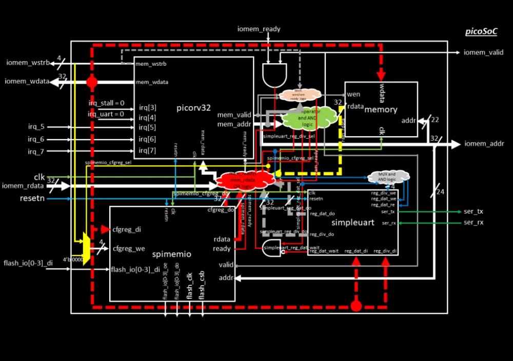
Chip floorplanning, macro placement, and robust power grid design to achieve optimal performance, power, and area.
Standard cell placement, clock tree synthesis, and detailed routing with timing and congestion optimization.
Multi-corner multi-mode timing closure, DRC/LVS, IR drop, EM analysis, and final GDSII signoff.
DESIGN SETUP & FLOORPLANNING
Technology setup, IO planning, macro placement, and power grid definition.
PLACEMENT & CLOCK TREE SYNTHESIS
Standard cell placement, clock tree synthesis, and timing-driven optimization.
ROUTING & TIMING CLOSURE
Global and detailed routing, ECOs, and multi-corner multi-mode timing closure.
PHYSICAL SIGNOFF
DRC, LVS, IR drop, EM analysis, and final GDSII tape-out signoff.